Workshop Scanning Electron Microscope (SEM)-2018
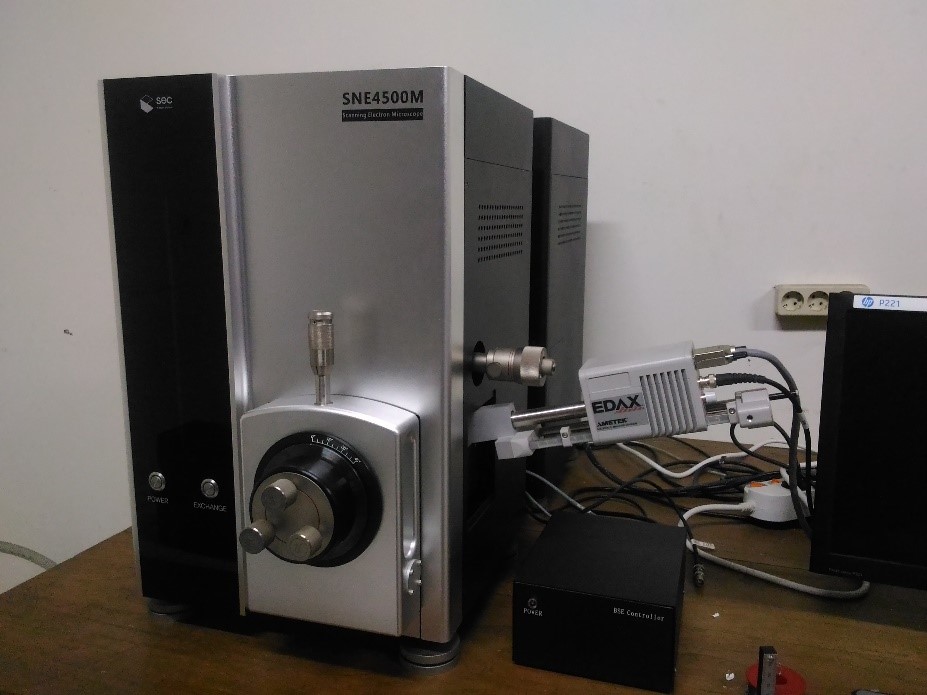
Scanning Electron Microscope (SEM) is a tool that has many benefits for analyzing the morphology and composition of a material. SEM is widely used in physics, biology, chemistry, and materials. The general working principle of SEM is that the filament generates the electron beam, the electron beam is focused using a magnetic lens, the electrons strike the sample, the detector captures the scattered electrons, and the surface morphology of the sample can be seen on the monitor screen. Two types of electrons can be detected: backscattered (BSE) and secondary (SE). BSE occurs when electrons hit the sample’s atoms elastically, while SE are electrons scattered due to inelastic collisions. When compared, BSE energy is greater than SE.
Samples that can be analyzed using SEM must be conductive. Non-conductive samples can also be tested using SEM after being coated with a conductor, usually gold (Au). Furthermore, the samples ready to be tested are placed in the reactor under vacuum conditions. The vacuum conditions usually used during SEM shooting are in the medium (10-3 Torr) to ultrahigh (10-10 Torr) range.
The Physics study program understands that in addition to mastering the concepts taught by lecturers to students in lectures, students need to be equipped with qualified experimental skills. The SEM Workshop is one of the study program development programs in the past two years.
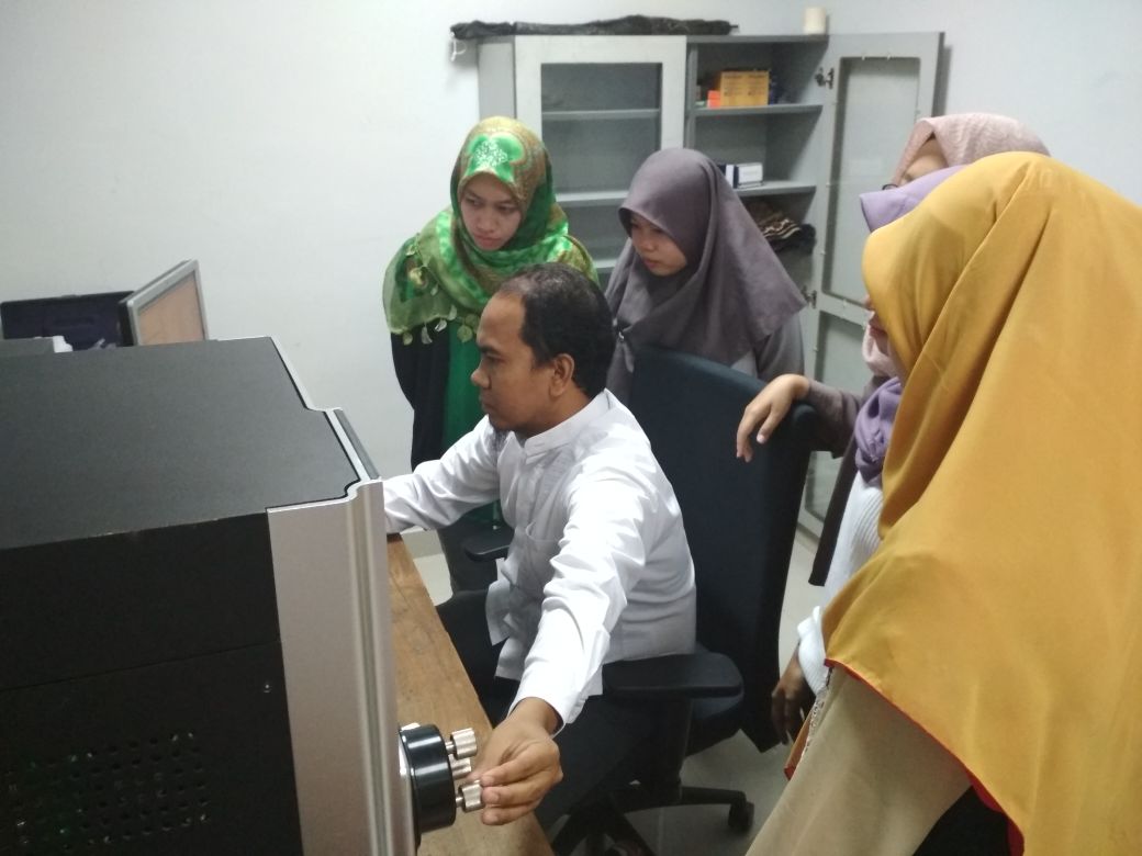
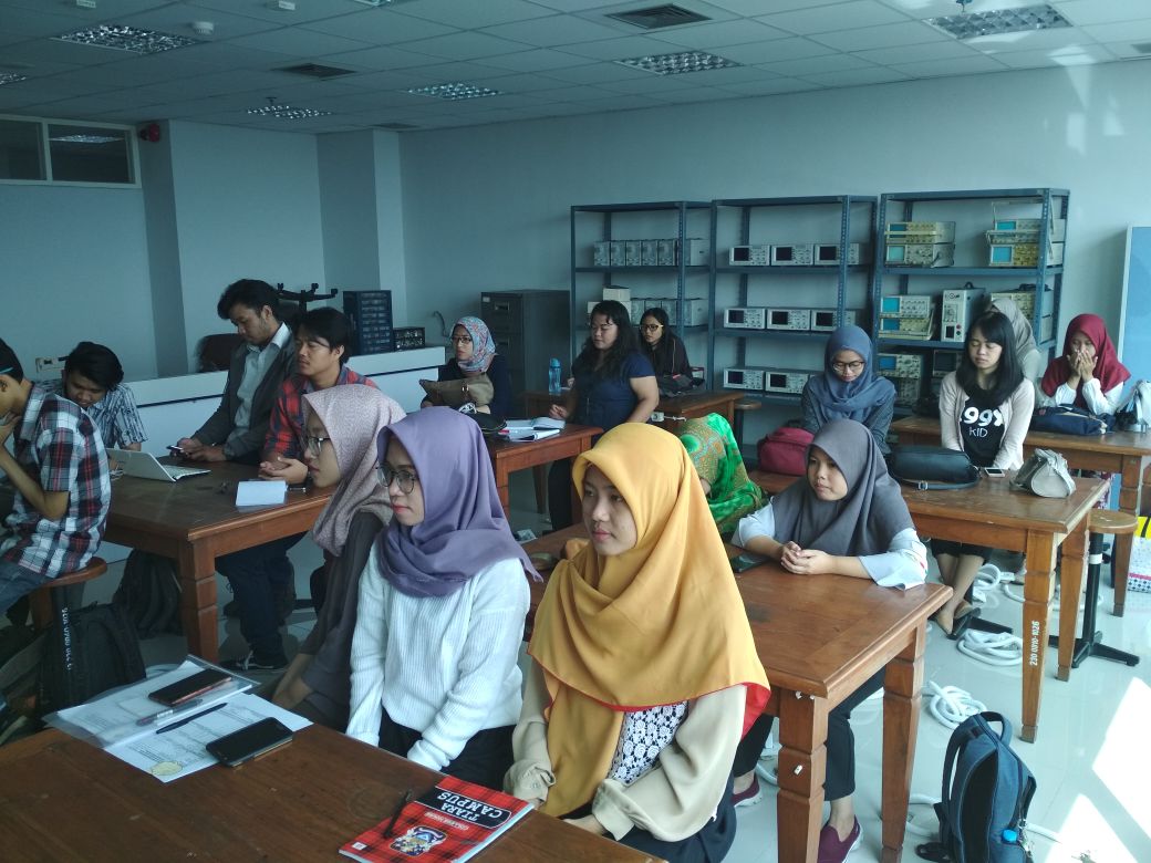
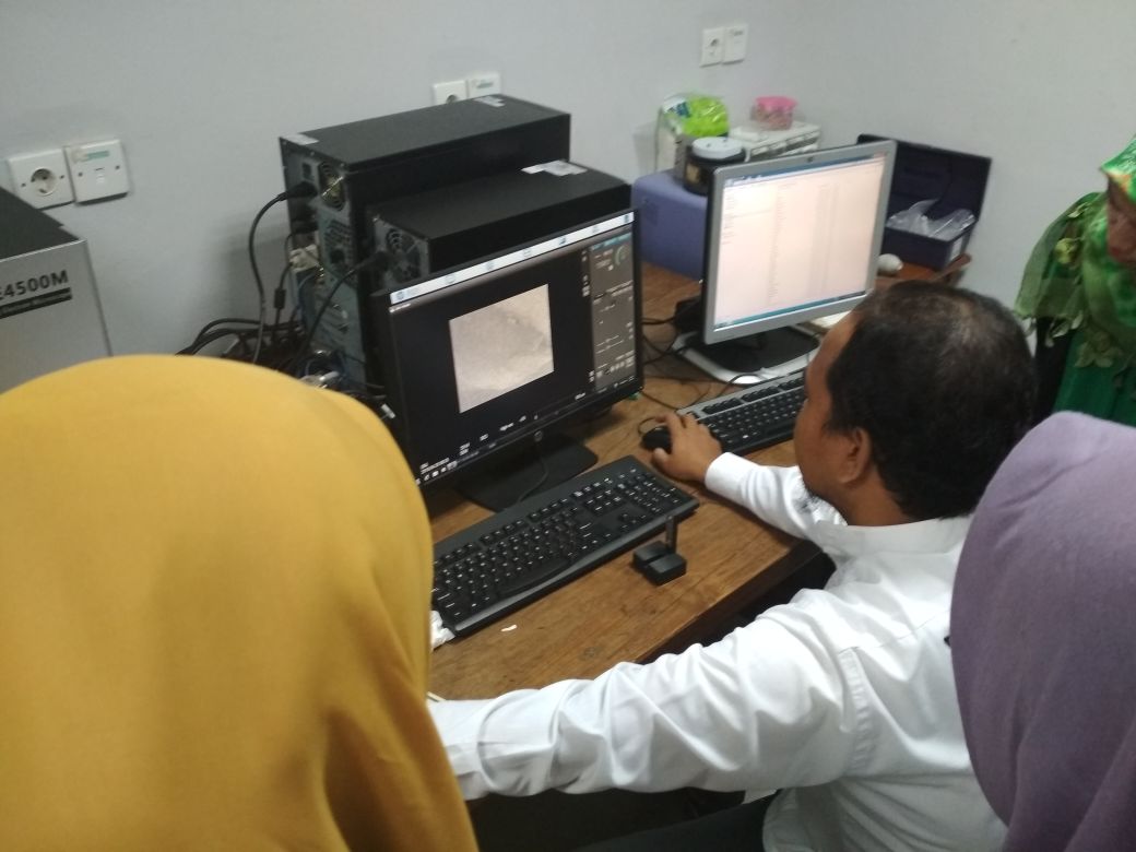
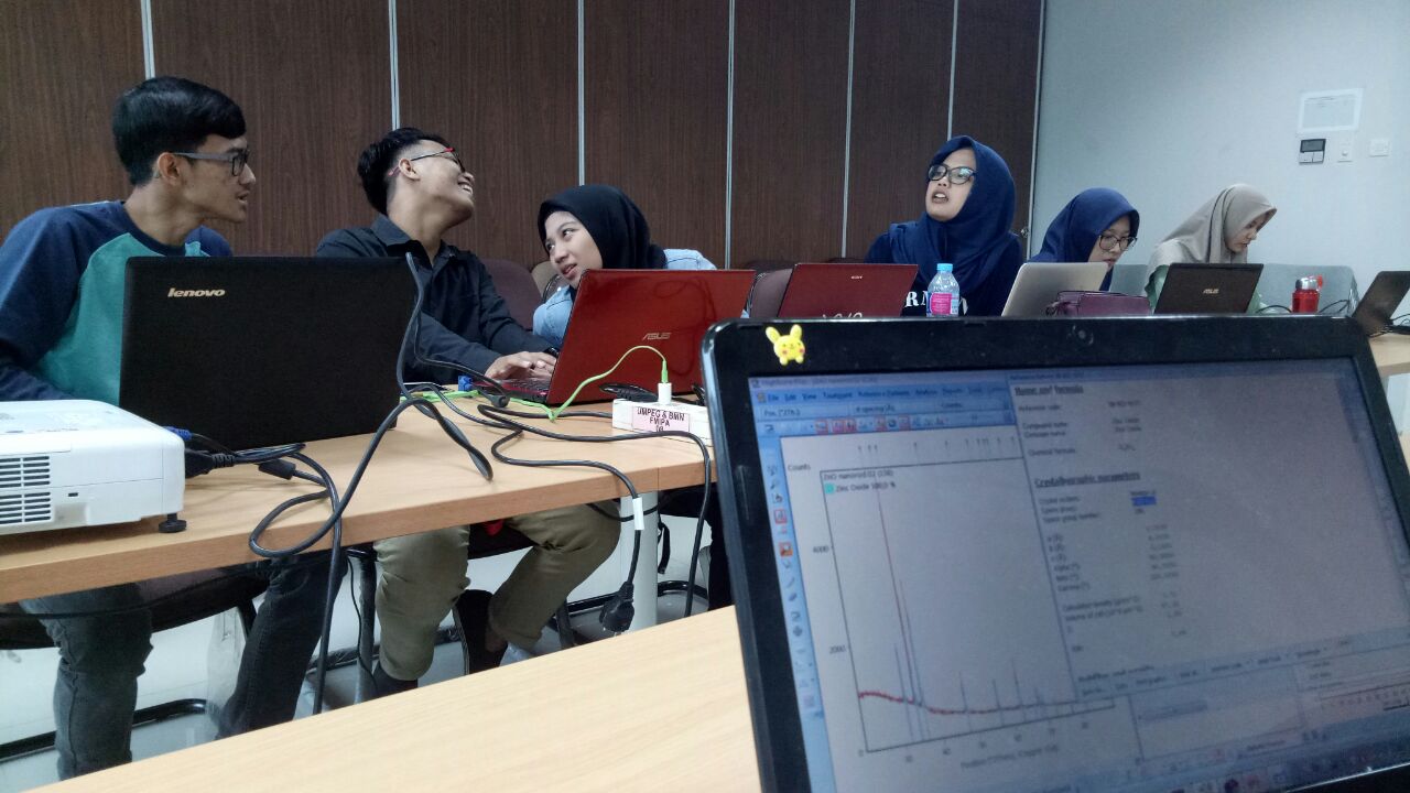
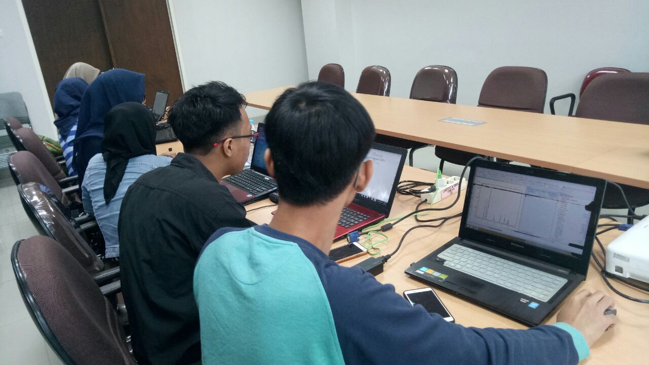
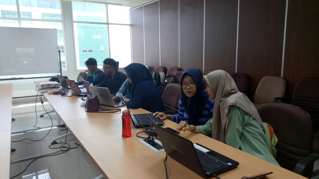
On April 20-21, 2018, the SEM workshop in the Physics study program was held for two days. On the first day, the workshop was opened by the head of the study program, Dr. Widyaningrum Indrasari, M.Si, and then the experimental group was guided by Mr. Fajrin. Students divided into small groups of 5 people are then guided using SEM by Mr. Fajrin, Education Laboratory Administrator. In the afternoon, at around 02.00 p.m., Mr. Dr. Iwan Sugihartono was a lecturer in the Physics study program with a research field in semiconductor materials. Providing material aims to make students understand how to carry out morphological, topographical, and compositional analyses of samples that have been analyzed using SEM. On the second day, students who had completed reports and understand SEM analysis presented their reports in front of examiners consisting of Dr. Iwan and Mr. Fajrin. (red: isugihar2018)