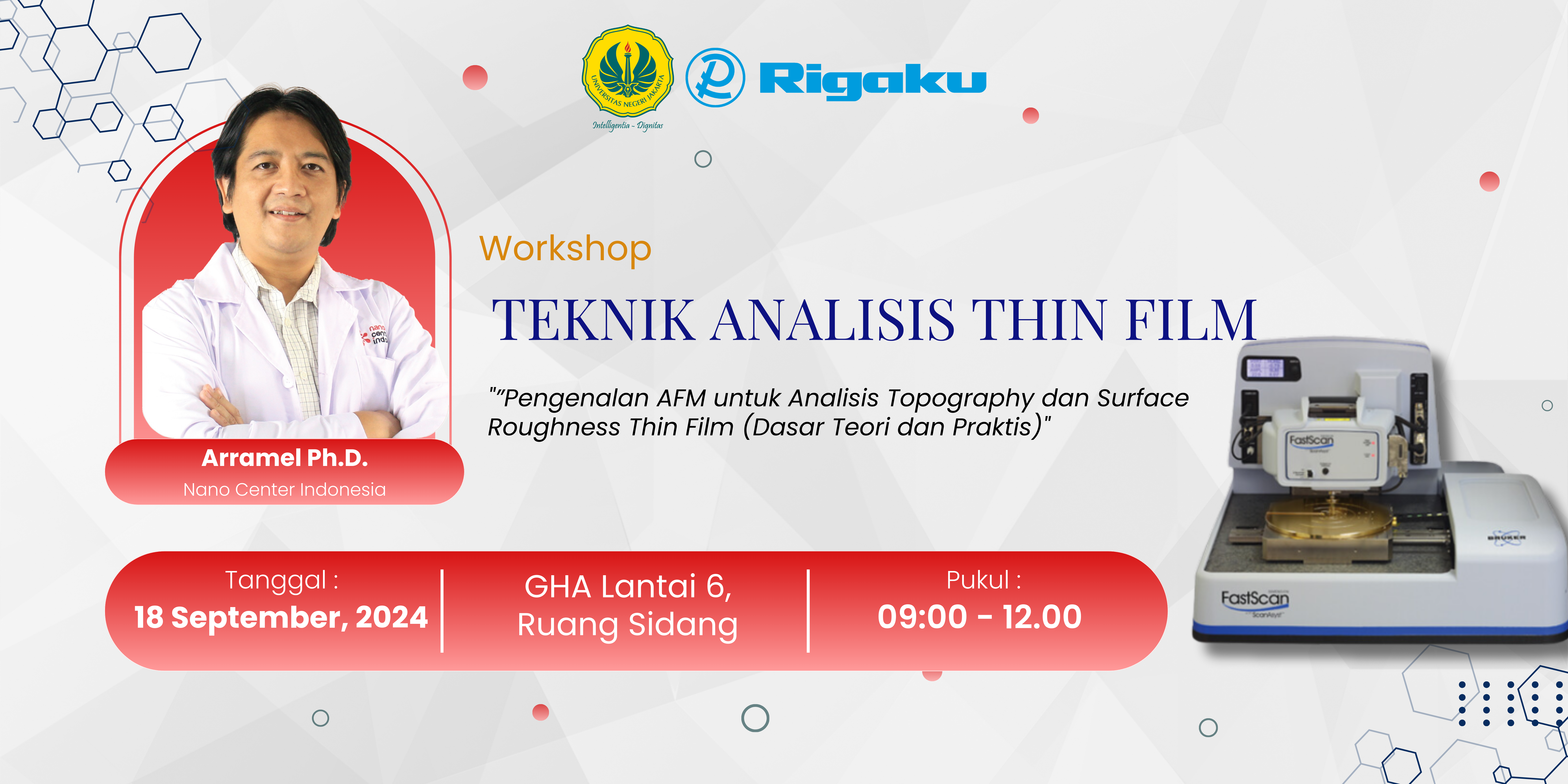
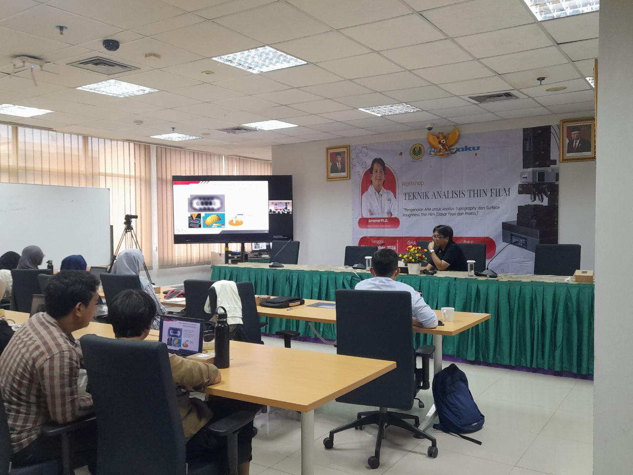
Chemistry Study Program at Universitas Negeri Jakarta (UNJ) collaborated with Nano Center Indonesia to successfully hold a workshop on material characterization methods focusing on the topic of “Introduction to AFM for Topography and Surface Roughness Analysis of Thin Films (Theoretical and Practical Fundamentals) on September 18, 2024, from 13:30 to 15:00 WIB. The event, which took place offline in the KH. Hasjim Asj’arie Building, featured an experienced speaker from Nano Center Indonesia, namely Arramel, Ph.D, an AFM instrument expert. This workshop was attended by 40 participants from the Chemistry Study Program, Classes of 2021 and 2022. The workshop facilitated students, especially those in the Chemistry Study Program, in enriching their experience and understanding of the basic concepts and analytical techniques of the Atomic Force Microscope (AFM) instrument. The series of events began with an opening, a prayer reading, and welcoming remarks from Prof. Dr. Setia Budi, M.Sc.
Dr. Arramel, Ph.D as the speaker, began the presentation by explaining the history and development of the AFM (Atomic Force Microscope) instrument from the concept of STM (Scanning Tunneling Microscope), which was discovered by Gerd Binnig and Heinrich Rohrer in 1981. The Scanning Tunneling Microscope uses the principle of quantum tunneling to obtain surface images at the atomic scale.
Next, participants were invited to delve deeper into the AFM instrument, which was invented in 1986. This instrument utilizes the interaction forces between a sharp probe tip and the sample surface to produce high-resolution topographic images. It operates in three main modes: contact mode, non-contact mode, and intermittent mode. Additionally, AFM can measure the mechanical, chemical, and electrical properties of a sample's surface, making it frequently used for thin film analysis due to its ability to image structures at the nanometer scale and measure surface roughness. Some advantages of AFM mentioned by the presenter include its non-destructive nature during measurements, the capability to produce high-resolution surface images, and its applicability to both conductive and non-conductive samples, resulting in a wide range of applications. After the presentation session, participants were encouraged to ask questions to the speaker to reinforce their understanding and create a more active interaction. The event concluded with the symbolic presentation of a certificate to the presenter and a documentation session.
With the successful organization of this workshop, it is hoped that students will be equipped with relevant knowledge and practical skills in the field of material chemistry, as well as prepare them to face challenges in the workforce and research. Furthermore, the collaboration between the Chemistry Study Program at UNJ and Nano Center Indonesia is expected to continue and make a tangible contribution to the development of science and technology in Indonesia.